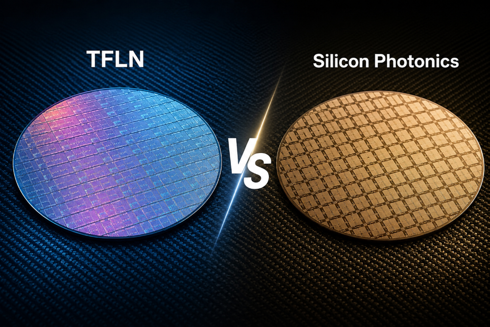
High-density AI networks are accelerating the transition from the 800G optical module to the 1.6T transceiver and future 3.2T optical engines. As GPU clusters scale, optical links must deliver more bandwidth per port while limiting power consumption, heat, and front-panel space.
Established technologies—including InP EMLs and silicon-photonics modulators based on free-carrier dispersion—remain important, but their performance must be balanced against bandwidth, drive-voltage, thermal, and packaging constraints at ultra-high baud rates. Silicon lacks a strong native Pockels effect, while higher-speed EML designs can add packaging-density and thermal-management pressure.
Among all materials, a TFLN modulator uses lithium niobate’s strong Pockels effect to enable high electro-optic bandwidth, low-voltage operation, and strong signal linearity. These characteristics make TFLN a promising platform for reducing the bandwidth and power-density bottlenecks facing next-generation optical transceiver designs.
What Is a TFLN Modulator?
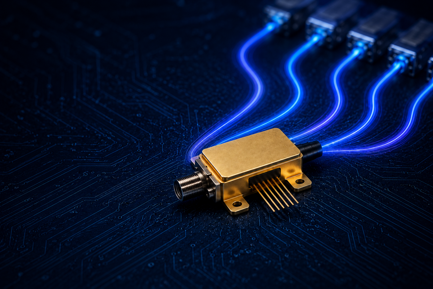
A TFLN modulator uses thin-film lithium niobate to convert electrical signals into high-speed optical signals. Lithium niobate is well suited to this task because it combines a strong Pockels effect, low optical loss, and a broad electro-optic response. Unlike silicon’s free-carrier approach, the Pockels effect changes refractive index linearly with an applied electric field, supporting efficient and highly linear modulation.
TFLN is also known as LNOI, or lithium niobate on insulator. It uses a thin lithium-niobate layer on an insulating substrate, rather than the much thicker crystal used in conventional bulk LiNbO3 modulators. This structure improves optical and RF field confinement, enabling shorter Mach-Zehnder modulator paths, tighter integration, and lower driving-voltage potential.
Why TFLN Matters for 200G–400G/Lane
l Low Vπ: A lower RF half-wave voltage reduces the driver-amplifier requirement and can help lower power consumption in high-speed optical transceiver designs.
l Wide EO bandwidth: Bandwidth above 60–70 GHz provides headroom for 200G-per-lane PAM4. Moving toward 400G per lane generally requires bandwidth beyond 100 GHz, together with optimized drivers, packaging, and equalization.
l Compact device footprint: Tighter optical confinement allows millimeter-scale modulation sections, supporting dense multi-channel photonic integrated circuits.
l Low insertion loss and high extinction ratio: These factors help preserve link budget and signal contrast in high-speed IMDD and coherent links.
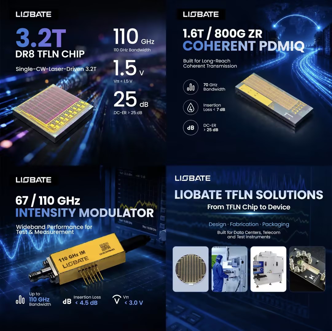
Liobate’s ultra-high-bandwidth TFLN intensity modulators are designed for wideband optical applications. Depending on the configuration, they provide a 3 dB electro-optic bandwidth of 63–105 GHz from 2 GHz, RF Vπ of 2.5–3.5 V, optical insertion loss of 5–6 dB, and a DC extinction ratio above 20 dB. These specifications support the performance, efficiency, and integration requirements of next-generation high-speed optical systems.
Role of TFLN Modulators in 800G Optical Modules
An 800G optical module can use different optical architectures for different reaches and fiber types.
l 800G SR8 is designed for short multimode-fiber links and typically uses eight parallel 100G PAM4 lanes.
l 800G DR8 uses eight 100G PAM4 lanes over single-mode fiber for short-reach data-center interconnects.
l 800G FR8 multiplexes eight 100G wavelengths onto duplex single-mode fiber for longer-reach links.
As 800G designs evolve toward fewer, faster lanes—such as four 200G PAM4 wavelengths—the modulator must handle higher baud rates while controlling power, heat, and RF packaging loss.
A TFLN Mach-Zehnder modulator (MZM) is well suited to this requirement. Its wide electro-optic bandwidth helps support approximately 100 GBaud-class PAM4 signaling for 200G-per-lane transmission, while its low Vπ can reduce the required driver voltage. TFLN’s linear Pockels-effect modulation can also support coherent-lite approaches that use amplitude and phase information to improve link performance or spectral efficiency.
Compared with silicon MZMs based on free-carrier dispersion, TFLN offers strong native electro-optic response, bandwidth headroom, and high linearity. Compared with EML and VCSEL solutions, it provides an external-modulation option that can be combined flexibly with laser sources and other photonic components.
These benefits are particularly relevant to Linear Drive Optics (LPO). LPO reduces in-module DSP retiming to lower power, so analog signal quality becomes more critical. The LPO MSA has released a 100G-per-lane specification for Ethernet links up to 800G and is targeting 200G-per-lane linear implementations. A wideband, low-voltage TFLN modulator can help make these next-generation 800G optical transceiver designs more practical.
From 1.6T to 3.2T Optical Engines
The next step is the 1.6T transceiver. One possible route uses eight 200G electrical or optical lanes, while other implementations may use more lower-speed lanes or different optical-engine architectures. The optimum approach depends on reach, form factor, thermal budget, DSP availability, and ecosystem readiness.
At 3.2T, designers increasingly consider 400G-per-lane operation. This is a major technical step because a 400G PAM4 lane may require approximately 200–224 GBaud-class signaling. The required electro-optic bandwidth, RF performance, driver capability, packaging precision, and power efficiency all become more demanding.
A 2026 technical report on 400G-per-lane photonic engines noted that TFLN can offer more than 100 GHz modulation bandwidth and low-voltage operation, characteristics that are highly relevant to high-baud-rate direct-detect and coherent applications.
This is where TFLN optical engines and optical interposer platforms become important. Rather than placing every photonic and electrical function in a conventional pluggable module, future systems may integrate lasers, TFLN modulators, silicon photonics routing circuits, photodetectors, and electrical interfaces across closely connected photonic subassemblies.
For data-center and HPC networks, the potential benefits include:
l Higher aggregate bandwidth within constrained front-panel space.
l Lower power per transmitted bit.
l Shorter electrical paths between switching silicon and optics.
l Better support for high-radix AI fabrics.
l Denser integration of multi-channel optical circuits.
l A potential path toward CPO and near-package optics.
Key TFLN Modulator Applications
TFLN modulators are relevant to several high-speed optical markets where bandwidth, energy efficiency, and signal quality are becoming critical design requirements.
1. Hyperscale Data Centers and Cloud Providers
Hyperscale operators need higher-capacity links for leaf-spine networks, storage fabrics, and large-scale AI infrastructure. TFLN can support the evolution from today’s 800G optical module toward the 1.6T transceiver and future 3.2T optical engines by enabling high-baud-rate PAM4 transmission with lower drive-voltage potential. This can help reduce power per bit and support greater bandwidth density in constrained switch and server environments.
2. AI/ML Clusters and Accelerator Fabrics
AI training and inference clusters generate intensive east-west traffic among GPUs, accelerators, switches, and memory resources. These architectures need low-latency, high-radix networks with scalable optical I/O. TFLN’s wide electro-optic bandwidth and linear modulation characteristics can support 200G-per-lane and emerging 400G-per-lane links, helping optical transceiver designers address the speed and power demands of next-generation accelerator fabrics.
3. Telecom and Metro Coherent Links
TFLN is also relevant to coherent optical transmission. Its linear electro-optic response and compatibility with MZM and IQ-modulator structures can support advanced modulation formats used in metro, data-center interconnect, and longer-reach transport links.
The potential for widespread adoption of TFLN modulators is strengthened by heterogeneous integration. A high-performance optical transceiver may combine TFLN modulation, silicon photonics routing, InP laser sources, photodiodes, and advanced packaging in one compact optical engine. Each platform can contribute what it does best rather than forcing one material system to perform every function.
Technical Challenges for TFLN Adoption
TFLN offers strong performance potential, but it must overcome several engineering and manufacturing challenges before broad high-volume adoption.
1. Integration and Packaging
High-speed modulation performance can be reduced by RF losses, impedance mismatch, wire-bond parasitics, fiber coupling loss, thermal stress, or package-level crosstalk. The modulator, driver, laser, passive photonic circuit, and package must be co-designed.
2. Wafer-Scale Manufacturing
Reliable TFLN production requires controlled thin-film bonding, lithography, etching, electrode processing, yield management, and wafer-level testing. Scaling from prototype devices to repeatable high-volume manufacturing is a central industry task.
3. Cost Structure
A new photonic platform must compete not only on performance but also on cost per port, supply-chain availability, assembly complexity, and testing time. The commercial value of TFLN will depend on whether its system-level power and performance benefits justify the total cost of ownership.
4. Thermal Management and Reliability
At 1.6T and 3.2T, heat generated by drivers, DSPs, switch ASICs, and optical components can become a system limitation. Long-term reliability must also be proven across temperature cycling, high-speed operation, humidity, optical power, and field deployment conditions.
Future Outlook for TFLN Photonics
1. Push Toward 400G per Lane and Beyond
The transition from 200G to 400G per lane is a critical step toward 3.2T optical transceivers and higher-capacity AI networks. It will require wider electro-optic bandwidth, lower drive voltage, better linearity, and stronger RF co-design. TFLN is attractive because its Pockels-effect modulation offers the performance headroom needed for ultra-high-baud-rate PAM4 and coherent-lite links.
2. Co-Packaged Optics and Optical Interposers
Co-packaged optics (CPO) moves optical engines closer to switch ASICs, reducing electrical trace length, loss, and power consumption. Optical interposers can integrate TFLN modulators with waveguides, laser coupling, photodetectors, and fiber interfaces. This creates a path toward compact, multi-channel optical engines for high-bandwidth AI switches, HPC systems, and future 3.2T interconnects.
3. Standardization and Ecosystem Maturation
TFLN adoption depends on more than device performance. The ecosystem needs interoperable specifications, qualified packaging, high-speed driver ICs, wafer-scale manufacturing, automated testing, and dependable supply chains. Currently, industry bodies (like OIF, IEEE, and COSA) are defining specs for TFLN-based optical engines, including footprint, RF pinouts, and driver interfaces.
4. Long-Term Outlook
TFLN is unlikely to replace silicon photonics, InP EMLs, or VCSELs across every optical link. Instead, these technologies will coexist based on reach, cost, wavelength, form factor, and integration needs. TFLN’s strongest long-term opportunity is in bandwidth- and power-constrained applications, including 1.6T and 3.2T engines, LPO, CPO, AI fabrics, and coherent interconnects.
Turning TFLN Potential into Practical Solutions
As the industry moves from 800G optical modules to 1.6T transceivers and future 3.2T optical engines, realizing the potential of TFLN requires more than strong material properties. It also requires coordinated chip design, wafer-scale fabrication, high-frequency packaging, optical coupling, and system-level engineering.
At Liobate, we focus on turning the high-bandwidth and low-voltage advantages of thin-film lithium niobate into practical photonic products for high-speed optical communications. Through our IDM model, we integrate TFLN PIC design, wafer-level manufacturing, device development, and packaging capabilities to support the development of reliable, scalable optical-interconnect solutions.
This integrated approach helps us optimize the parameters that matter most in high-speed applications, including electro-optic bandwidth, Vπ, optical insertion loss, extinction ratio, RF electrode performance, fiber coupling, package configuration, and long-term reliability.
Our TFLN portfolio supports applications ranging from 800G data-center interconnects to 1.6T and 3.2T optical-engine development, as well as coherent communications, microwave photonics, sensing, and test applications.
| Product category | Liobate solutions | Application focus |
| Data-center TFLN chips | 800G DR8/DR4 and 1.6T DR8/DR4 chip solutions | High-speed data-center interconnects, AI clusters, cloud networks, and multi-channel optical engines |
| 3.2T optical-interconnect chips | 3.2T DR8 TFLN chip solutions | Future 3.2T optical engines, hyperscale AI infrastructure, and high-density optical I/O |
| Coherent TFLN chips | 128 GBaud PDMIQ chip solutions | Coherent optical communications, data-center interconnect, metro networks, and telecom transport |
| Ultra-high-bandwidth TFLN chips | TFLN chip platforms supporting bandwidths above 130 GHz | Advanced optical communications, high-baud-rate modulation, microwave photonics, and test applications |
| TFLN intensity modulators | 40G, 67G, and 110G intensity modulator options | Optical communications, analog photonics, optical computing, sensing, and laser modulation |
| TFLN IQ and phase modulators | 40G/70G IQ modulators and 40G phase modulators | Coherent modulation, amplitude and phase control, interferometric sensing, LiDAR, and quantum-photonic research |
| Laser and frequency-comb solutions | Ultra-narrow-linewidth swept lasers and optical frequency-comb products | FMCW LiDAR, precision measurement, sensing, spectroscopy, and advanced photonic systems |
Work with Liobate
Whether you are developing an 800G optical module, evaluating a 1.6T transceiver architecture, planning a 3.2T optical engine, or exploring a custom TFLN photonic solution, contact Liobate to discuss your project requirements.
Our team can help identify suitable products or develop customized solutions based on your target bandwidth, operating wavelength, modulation format, drive-voltage range, package configuration, fiber coupling requirements, and end-use environment.


 The previous article
 Returns the list

 2026/11/11