Large language models (LLMs) and generative AI workloads are driving a rapid rise in training and inference demand. The 2025 Stanford AI Index reports that training compute for notable models is doubling about every five months. As more data moves between processors, memory, and accelerators, copper interconnects face speed, heat, and power limits. Integrated photonics offers another path by moving and processing data with light, while the TFLN modulator provides the high-speed electro-optic interface that makes this shift practical.
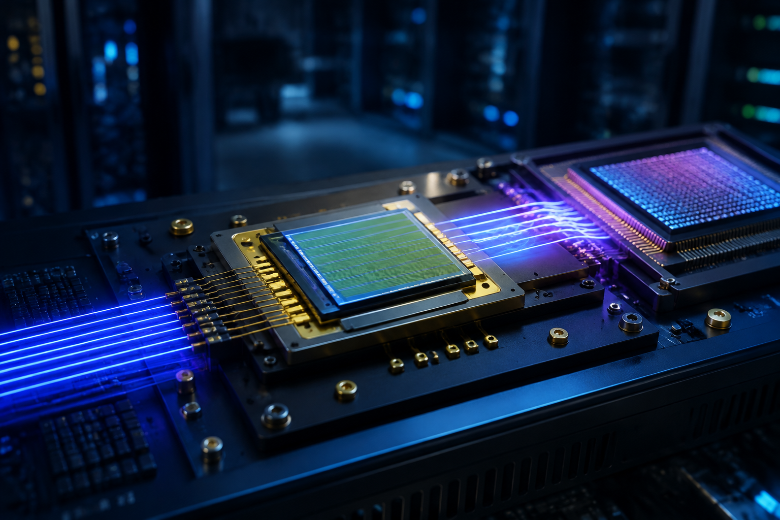
What Are TFLN Modulators in Photonic Computing?
Thin-film lithium niobate (TFLN) modulators are high-speed electro-optic modulators that translate an electrical signal into a controlled change in optical intensity or phase.
In TFLN, an applied electric field alters the refractive index through the Pockels effect, allowing the optical waveform to be modulated in phase and, via interference, in intensity to follow the electrical input. Thin-film waveguides concentrate optical and RF fields in a compact photonic chip, supporting broad bandwidth, low optical loss, and low drive voltage.
That conversion function makes a TFLN modulator a core building block for three system classes:
l Photonic links. It encodes high-rate electrical data onto an optical carrier for movement between chips, boards, or racks.
l AI accelerators. It maps inputs and weights into optical amplitude or phase for parallel multiply-and-accumulate operations.
l Quantum systems. It provides fast, precise intensity or phase control for state preparation, routing, and readout architectures.
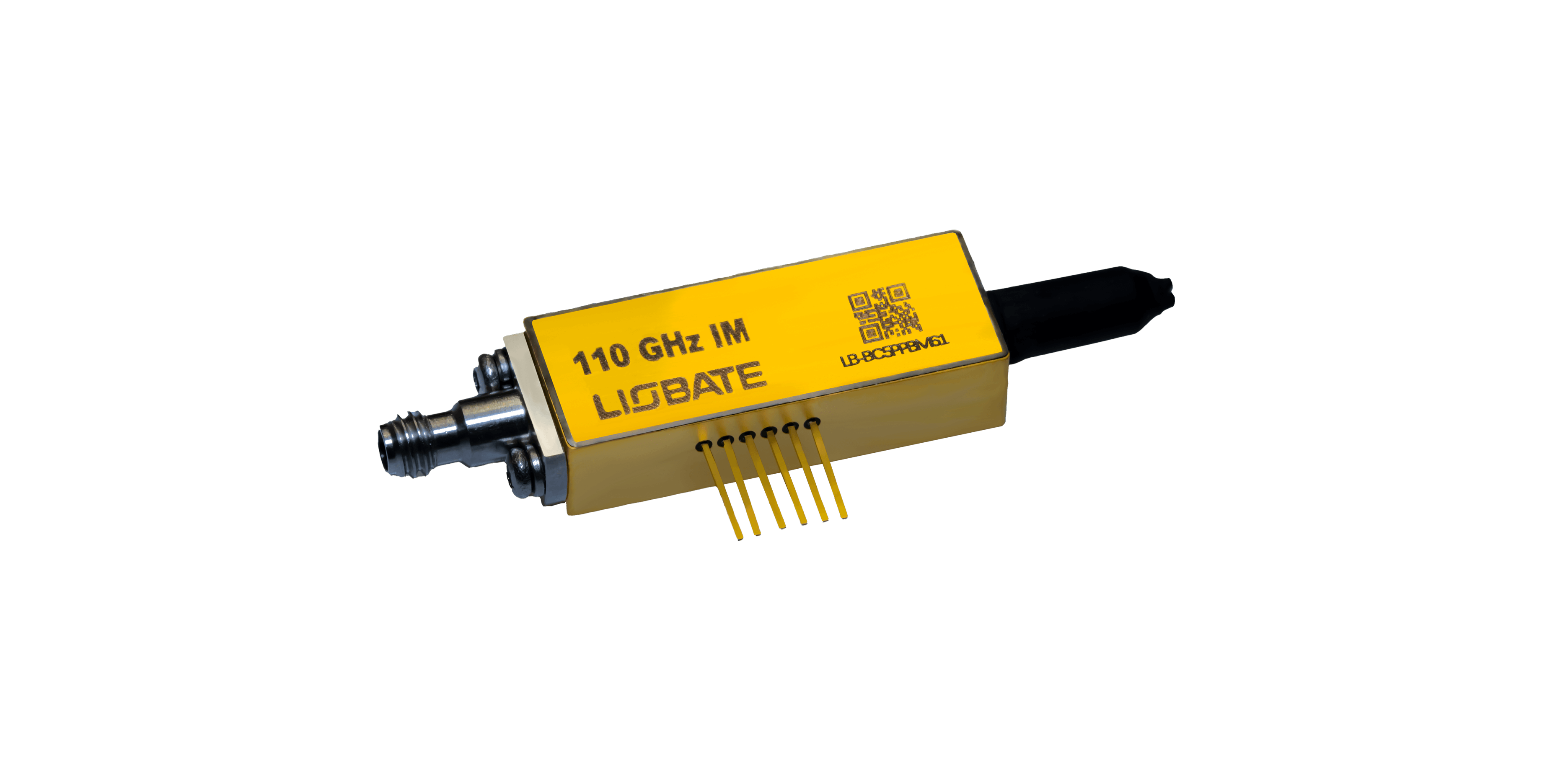
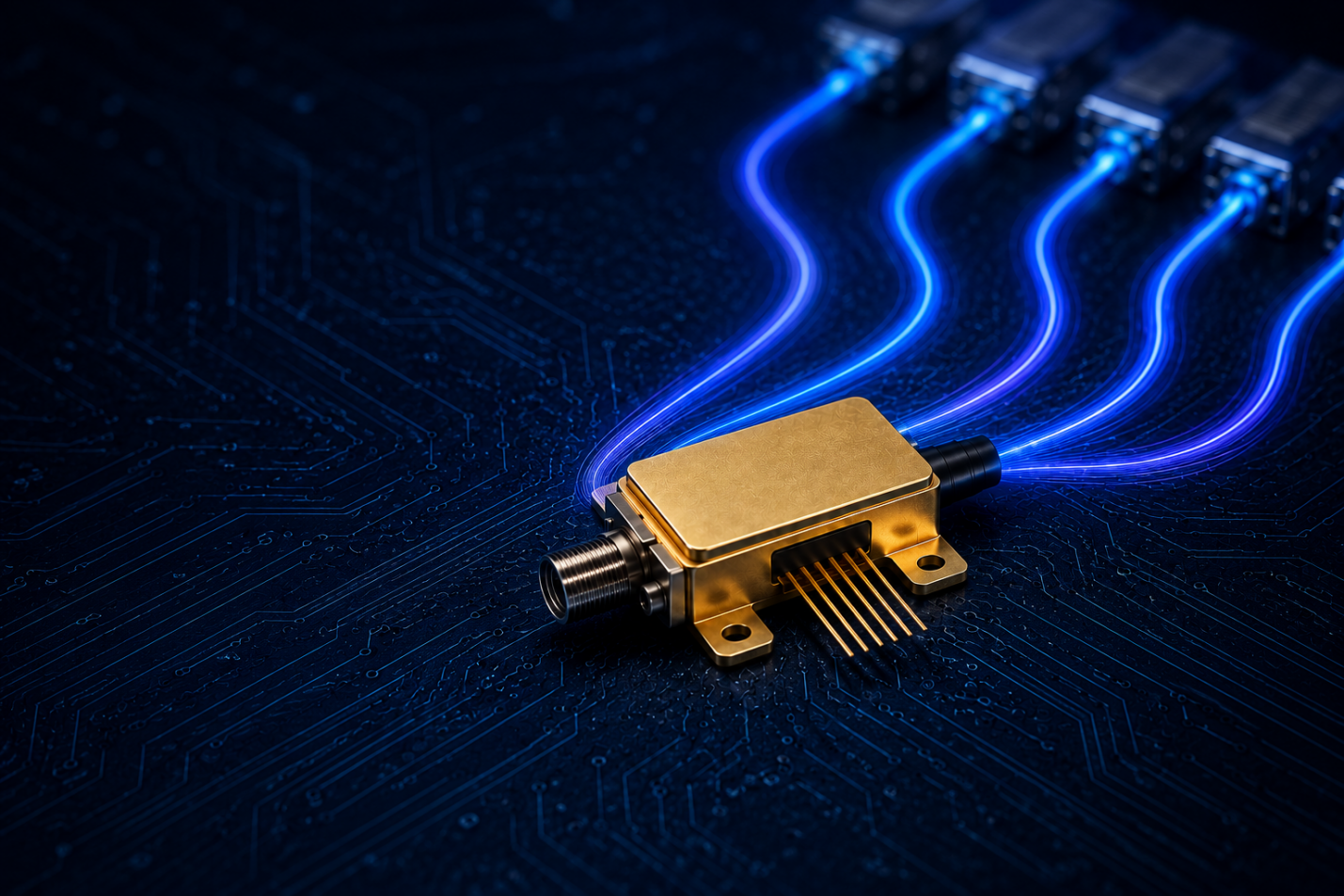
Liobate 110 GHz TFLN intensity modulator for high-speed electro-optic conversion
How Do TFLN Modulators Improve Photonic Computing Performance?
TFLN improves compute performance where electronic data enters and controls the optical core. Three related capabilities determine how much useful work the photonic fabric can deliver:
1. Ultra-High Bandwidth Accelerates Data and Weight Updates
Bandwidth determines how quickly optical inputs and weights can change. A 2024 Nature Communications demonstration reached 120 GOPS with a 60 GHz weight-update speed in a TFLN tensor core. Faster updates support high-rate inference and in-situ learning without leaving the optical core idle.
2. Dense Integration Builds Parallel, Programmable Cores
Thin-film waveguides place modulators beside splitters, interferometers, resonators, and routing elements on the same photonic chip. Multiple optical channels can then operate in parallel through wavelength, time, or spatial multiplexing. Shorter paths and fewer fiber-connected components make the compute core denser and easier to reconfigure.
3. Linear, Low-Noise Modulation Preserves Analog Signal Quality
Photonic AI operations often represent numbers as optical amplitude or phase. A linear response keeps the optical signal proportional to the intended input or weight, while low noise preserves useful precision across cascaded operations. This supports more faithful matrix-vector multiplication and more predictable calibration.
Together, these properties let a photonic compute fabric combine high throughput with the flexibility to adapt inputs, weights, and network dimensions.
How Do TFLN Modulators Improve Power Efficiency?
Power efficiency improves when the electro-optic interface uses less energy per bit and the optical path replaces part of the electrical data-movement chain. The system impact is increasingly important: global data-center electricity use was about 415 TWh in 2024 and is projected to reach around 945 TWh by 2030. Against this backdrop, TFLN contributes through two mechanisms:
l Lower energy per bit. The Pockels effect changes the refractive index directly, enabling fast modulation with low drive voltage and low optical loss. This reduces driver demand and the laser power needed to overcome optical loss.
l Fewer ohmic losses in the interconnect. Once data enters the optical domain, light can carry and fan out signals without the same resistive and capacitive losses as a copper segment. Optical multiplexing also carries several channels through shared waveguides.
A 2025 Nature Communications study demonstrated 43.8 GOPS per channel at 0.0576 pJ per operation on an integrated TFLN circuit. The result shows how efficient modulation, low-loss routing, and optical fan-out can work together, rather than treating each device as an isolated component.
At chip level, this reduces driver and laser overhead and lowers energy per operation. At rack level, optical links can reduce transport power and the heat added by data movement. TFLN therefore addresses both budgets through the same high-speed optical interface.
TFLN Modulator Manufacturing, Integration, and Ecosystem Readiness
Readiness depends on more than a fast electro-optic modulator. Photonic computing moves toward deployable hardware only when materials, fabrication, packaging, electronics, and software operate as one repeatable system.
Heterogeneous Integration Combines Specialized Materials
TFLN provides efficient modulation and low-loss routing. Silicon and silicon nitride contribute passive circuitry, III-V materials add lasers and detectors, and CMOS supplies memory, drivers, converters, and control logic. Heterogeneous integration combines these strengths without forcing one material to perform every function.
Wafer-Scale Manufacturing Builds Ecosystem Momentum
Wafer-scale processing, automated testing, and foundry-oriented workflows are moving TFLN beyond one-off prototypes. Shared design rules, yield control, and repeatable packaging give designers a more stable path from circuit layout to manufactured device.
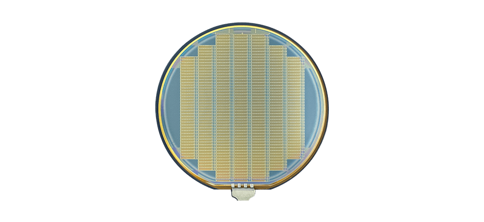
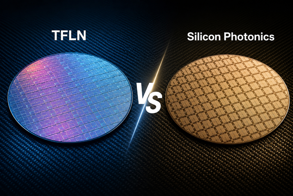
Patterned TFLN wafer supporting scalable photonic chip manufacturing at Liobate
System-Level Co-Design Turns Devices into Compute Engines
A working engine must align modulation with lasers, photodetectors, RF drivers, DACs and ADCs, bias control, thermal management, and calibration software. The package must preserve optical loss, electrical bandwidth, and signal quality across every interface. System-level co-design turns a group of fast devices into a stable accelerator subsystem.
When these layers are coordinated, the photonic chip becomes a manufacturable subsystem rather than a collection of individually fast devices. This is where a full-chain TFLN partner adds practical value.
Advance Photonic Computing with Liobate TFLN Solutions
Liobate brings these layers together through an IDM platform covering TFLN chip design, wafer fabrication, testing, and device packaging. This full-chain workflow keeps optical performance, RF interfaces, channel density, and package constraints connected throughout development.
For photonic computing programs, our support is organized around three connected layers:
l Device foundations for optical encoding. Our comprehensive TFLN device portfolio provides intensity and phase modulation options for high-speed optical encoding.
l Integrated PIC architectures for parallel processing. Liobate's PIC integration capabilities combine passive devices with multi-channel high-speed electro-optic modulation, supporting parallel optical paths and custom channel architectures.
l Packaging and co-development for system integration. Low and repeatable fiber coupling, wide electrical bandwidth, and hybrid integration with lasers or detectors help preserve chip performance in the packaged device. Custom chip and package development can align channel count, interfaces, and form factor with the target system.

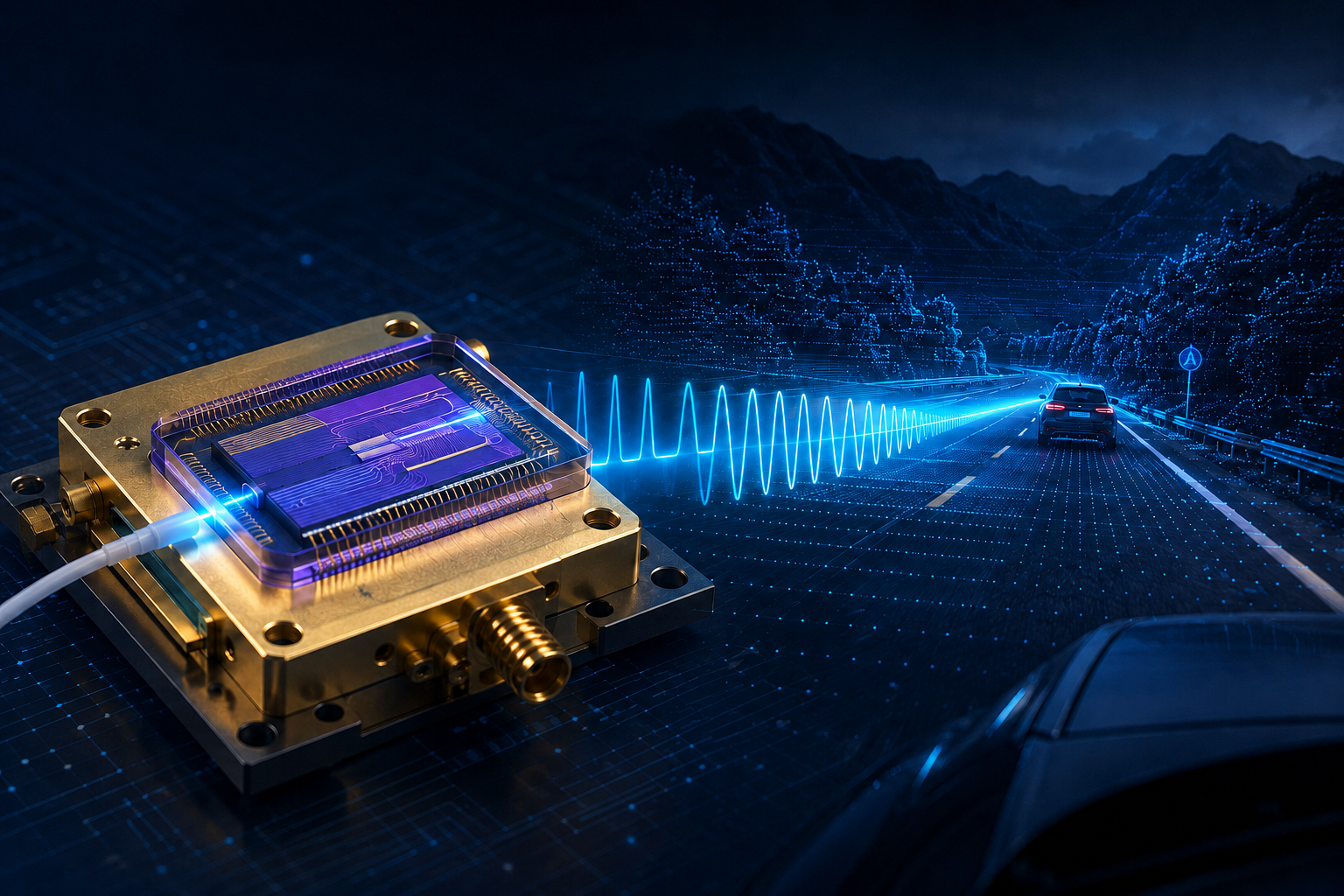
Liobate packaged TFLN modulator with optical and electrical interfaces
This combination allows photonic computing teams to evaluate the modulator, PIC, and package as one design problem. Teams developing a photonic chip, optical AI accelerator, or high-bandwidth interconnect can contact us to discuss the required modulation function, channel architecture, interfaces, and packaging approach.


 The previous article
 Returns the list
 2026/11/11