Silicon photonics and thin-film lithium niobate are two important platforms for next-generation optical systems. Silicon photonics is already widely used in high-volume data-center interconnects because of its mature manufacturing ecosystem and high integration density. TFLN, by comparison, is gaining attention for high-speed, low-loss, and highly linear electro-optic modulation.
Choosing between them isn't a matter of which is "better" overall — it depends on your bandwidth targets, power budget, and manufacturing readiness. This article compares TFLN and silicon photonics across the metrics that matter, then offers practical guidance on which platform fits which application.
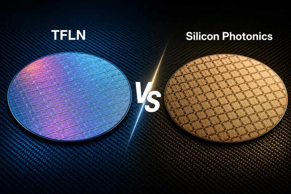
What Are TFLN and Silicon Photonics?
1. What Is TFLN?
Thin-film lithium niobate, commonly abbreviated as TFLN, is also known as lithium niobate on insulator, or LNOI. It consists of a thin single-crystal lithium niobate layer bonded to an insulating layer and a supporting substrate.
The lithium niobate film is typically 300-700 nanometers thick. This structure confines light much more tightly than traditional bulk lithium niobate devices, allowing smaller waveguides, stronger interaction between electrical and optical fields, and more compact modulators.
The main advantage of TFLN photonics comes from lithium niobate’s linear Pockels effect. An applied electrical field changes the material’s refractive index quickly and predictably, making TFLN well suited to Mach–Zehnder modulators, phase modulators, coherent transmitters, microwave photonic links, and precision sensing systems.
Important TFLN characteristics include:
Electro-optic bandwidths that can exceed 100 GHz in suitable modulator designs
Low drive-voltage potential
Low optical propagation loss
High linearity for analog signal processing
A broad optical transparency window
Strong second-order nonlinear optical properties
Good tolerance of relatively high optical power
Representative companies participating in the TFLN ecosystem include Liobate, HyperLight, Lightium, and other chip, foundry, packaging, and wafer suppliers. The ecosystem is expanding, although it remains less mature than the global silicon photonics supply chain.
2. What Is Silicon Photonics?
Silicon photonics uses semiconductor fabrication methods to create optical components on silicon-based wafers, usually silicon-on-insulator platforms.
A silicon photonic integrated circuit can contain waveguides, splitters, filters, multiplexers, modulators, germanium photodetectors, couplers, and thermal tuning elements. Silicon’s high refractive-index contrast enables tight bends and compact optical routing, supporting very dense integration.
Silicon photonics is especially valuable because it can use established semiconductor manufacturing infrastructure. Foundries can provide standardized process design kits, multi-project wafer services, automated production, and mature packaging workflows.
Its limitations come mainly from the material itself. Silicon does not have a strong native Pockels effect, so most silicon modulators depend on carrier depletion, carrier injection, or resonant modulation mechanisms. These approaches can deliver high performance, but designers must balance bandwidth, drive voltage, optical loss, thermal sensitivity, and linearity.
Major silicon photonics participants include integrated device manufacturers, semiconductor foundries, optical component suppliers, and cloud or networking companies. The ecosystem includes companies such as Intel, GlobalFoundries, TSMC, Tower Semiconductor, Cisco, Marvell, and numerous transceiver and packaging suppliers.
TFLN vs Silicon Photonics: A Comprehensive Comparison
Neither technology is universally superior. Each offers a different combination of speed, integration, cost, and production readiness.
| Comparison Area | TFLN Photonics | Silicon Photonics |
|---|---|---|
| Modulation mechanism | Linear electro-optic Pockels effect | Usually based on carrier depletion, carrier injection, or resonant tuning |
| High-speed potential | Particularly strong for very high baud-rate modulation | Strong for mainstream datacom, but performance depends heavily on modulator architecture |
| Drive efficiency | Can support relatively low drive voltage while maintaining high speed | May require greater trade-offs between voltage, bandwidth, and optical loss |
| Optical loss | Potentially very low in optimized waveguides | Compact routing is excellent, although active silicon structures can introduce additional loss |
| Linearity | Well suited for analog and microwave photonics applications | Device-dependent and generally more challenging for highly linear analog links |
| Integration density | Lower than silicon for dense passive routing | Very high due to tight optical confinement and small bend radii |
| Manufacturing maturity | Developing rapidly, with growing 150 mm and 200 mm wafer capabilities | Highly mature, with established CMOS-compatible foundry infrastructure |
| Manufacturing cost | Generally higher at present | More competitive for high-volume production |
| DC bias stability | Historically prone to drift; now solved through heterogeneous integration | Excellent |
| High-power handling | Strong potential because TFLN avoids silicon’s telecom-band two-photon absorption effects | High optical power may cause two-photon absorption and free-carrier absorption |
| Best-fit applications | Coherent optics, microwave photonics, RF-over-fiber, sensing, and very-high-speed modulation | High-volume optical transceivers, co-packaged optics (CPO), optical switching, and dense photonic integration |
Application Scenarios: Which to Choose Between TFLN and Silicon Photonics?
1. Choose Silicon Photonics When:
• High-Volume and Cost-Sensitive Production Is the Priority
Silicon photonics is a practical choice for short- and medium-reach data-center interconnects where manufacturing scale, price per transmitted bit, and multi-source availability are critical.
Its established wafer and packaging ecosystem can support standardized optical engines, transceivers, and high-density switching platforms.
• A Mature Supply Chain Is Required
Projects with strict qualification schedules, high annual volume, or limited tolerance for process risk may benefit from silicon photonics. Designers can access established foundries, process design kits, testing infrastructure, and electronics integration options.
• High-Density Integration Is Critical
Silicon photonics is well suited to co-packaged optics, dense wavelength-division multiplexing, optical I/O, and systems that must integrate many passive and active functions close to a switch ASIC or computing processor.
2. Choose TFLN When:
• Ultra-High Baud Rate Is Required
TFLN is a strong candidate for high-baud-rate coherent transmitters, next-generation 1.6T and 3.2T modules, and applications seeking to increase per-lane capacity without continually adding parallel channels.
The practical value is not simply a higher bandwidth number. Greater modulator bandwidth can improve signal integrity, reduce equalization pressure, and give system architects more flexibility when choosing modulation formats.
• Low Loss and High Linearity Matter
TFLN is particularly relevant to analog photonics, microwave photonics, radar, RF-over-fiber, optical sensing, frequency conversion, and laboratory measurement systems.
Its linear electro-optic response can preserve signal fidelity across a wide dynamic range, while low optical loss helps maintain link margin.
• High-Speed Power Efficiency Is a Priority
AI and machine-learning clusters must increase interconnect capacity without allowing optical-engine power to grow at the same rate. A low-voltage TFLN modulator may reduce driver requirements and improve transmitter efficiency, especially in very-high-speed lanes.
The benefit should still be validated at module level, including DSP, laser, packaging, and thermal-control power.
3. Consider a Hybrid TFLN-on-Silicon Approach
For many products, the best answer is not TFLN or silicon photonics alone.
A heterogeneous architecture can use silicon or silicon nitride for compact waveguide routing, multiplexing, coupling, germanium detection, and electronic integration. TFLN is added where high-speed and low-voltage modulation create the greatest system benefit.
Possible integration methods include wafer-level bonding, die bonding, back-end integration, and micro-transfer printing. The preferred route depends on production volume, thermal budget, alignment tolerance, optical transition loss, wafer size, and packaging strategy.
This approach allows manufacturers to retain the scalability of silicon photonics while introducing TFLN only in the performance-critical sections of the optical engine.
Liobate’s Advantages in TFLN Technology
Founded in 2020, Liobate focuses on advancing thin-film lithium niobate (TFLN) photonics through an integrated development approach that covers chip design, wafer fabrication on 6-inch and 8-inch platforms, and in-house packaging. This IDM model enables closer control over the entire development process, from photonic device design to packaged optical solutions.
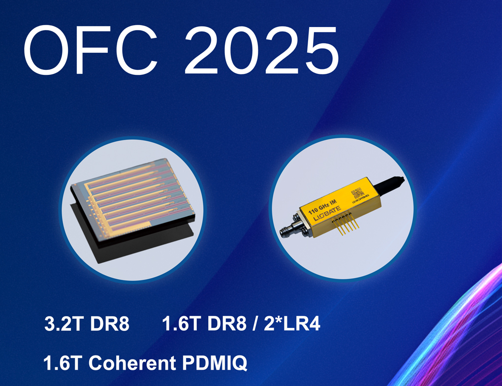
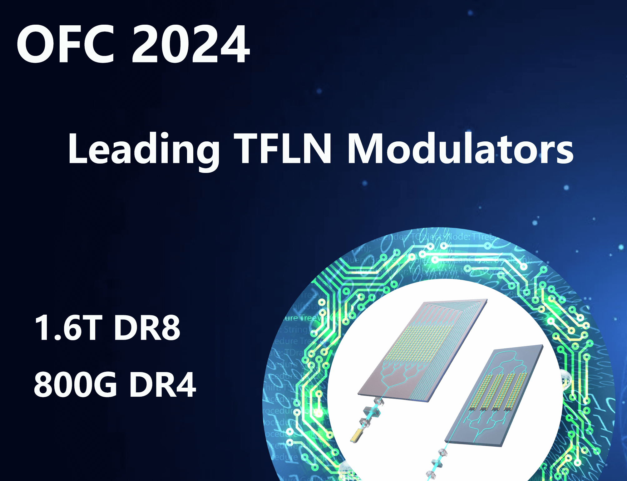
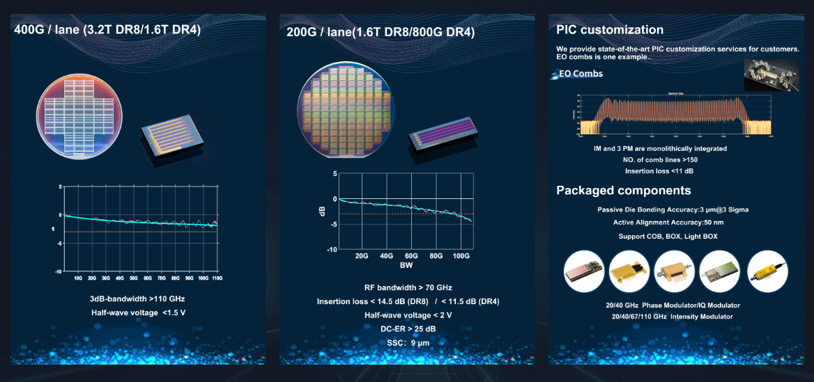
Liobate’s TFLN product portfolio includes high-speed optical modulators and photonic chips designed for next-generation optical communication systems. Key products include the 3.2T DR8 chip featuring up to 110 GHz bandwidth, insertion loss below 14 dB, and differential half-wave voltage below 1.5 V; the 1.6T DR8/800G DR4 chip with 70 GHz bandwidth; and the 1.6T/800G ZR coherent PDMIQ chip for long-haul transmission applications. Liobate also provides standalone intensity modulator dies with bandwidths reaching 110 GHz and insertion loss below 5 dB.
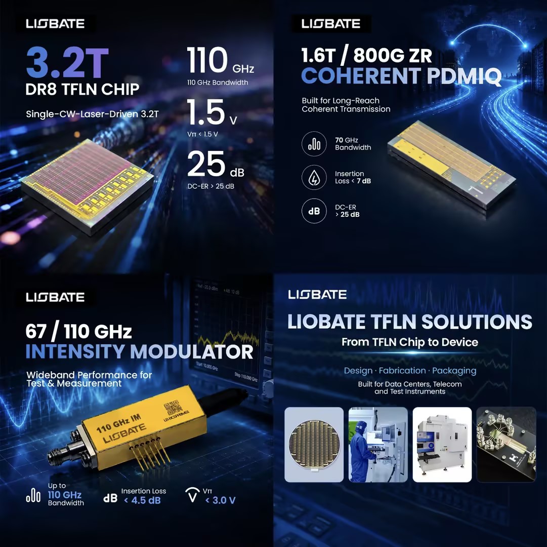
Beyond achieving high-speed modulation performance, Liobate has focused on improving the long-term stability of TFLN devices by addressing challenges such as DC bias drift through proprietary process optimization.
By combining high bandwidth, low drive voltage, and improved operational stability, Liobate’s TFLN solutions are designed to support a wide range of emerging applications, including AI-driven data centers, optical communications, test and measurement systems, and autonomous-driving LiDAR.
Whether you are developing next-generation optical networks or exploring customized photonic solutions, reach out to Liobate’s technical team to learn how TFLN technology can support your application needs!


 The previous article
 Returns the list

 2026/04/15
 ![What Is Thin Film Lithium Niobate (TFLN)? [2026 Guide]](/uploads/images/20260127/da49741612e7efa688d5688e3aad4562.png)