Engineers frequently investigate how light interacts with matter to improve high-speed data transmission systems. At Liobate, we examine the fundamental physics that allow tfln chips to outperform legacy materials in complex optical environments. By refining how we manipulate light at the micro-scale, we provide technical solutions that address the scaling hurdles common in both autonomous driving and high-speed communication networks.
The Material Advantage in Modern Photonics
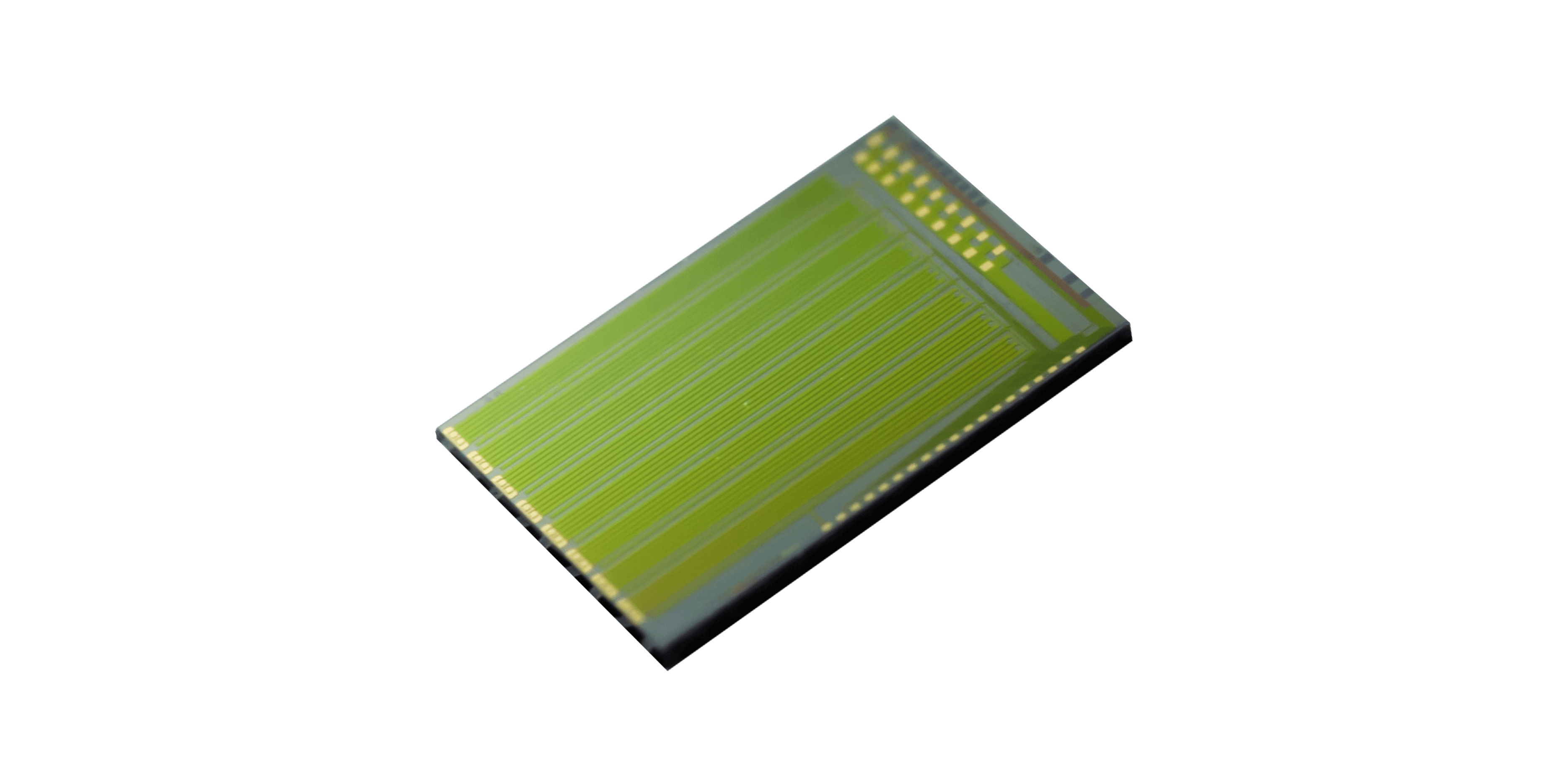
Our focus centers on the unique properties of thin-film lithium niobate, which serves as the foundation for our high-performance TFLN photonic chip designs. Unlike traditional bulk materials that often struggle with large footprints and high power consumption, this thin-film approach utilizes a high Pockels coefficient to achieve efficient electro-optic modulation. We find that the ability to confine optical fields within compact waveguides significantly reduces the half-wave voltage, often to sub-volt levels. This reduction is vital for our customers, as it allows for direct integration with standard CMOS electronics without requiring power-hungry RF drivers.
When we develop these components, our goal is to maintain signal integrity while maximizing throughput. Real-world measurements from our product portfolio show that we can achieve bandwidths exceeding 110 GHz with insertion loss figures below 14 dB for our high-performance modules. These metrics demonstrate how precise control over the refractive index and material geometry allows us to solve the classic trade-off between device size and operational speed.
Addressing Technical Challenges Through Precision Engineering
Technical challenges in fields like autonomous driving demand robust hardware that remains stable under varying temperatures and environmental stressors. We observe that the high linearity and thermal stability of our tfln chips make them ideal for sensing applications, including solid-state beam steering for LiDAR systems. By eliminating mechanical moving parts, these solutions offer the long-range, high-resolution sensing required for reliable environment mapping.
Furthermore, the design of our TFLN photonic chip architecture emphasizes scalability and manufacturability. We have transitioned our fabrication processes to utilize larger wafer sizes, ensuring that the components we provide can meet the volume requirements of modern industrial deployments. This shift not only lowers the cost per die but also ensures that the performance gains we observe in laboratory settings are replicable in mass production. Our proprietary fabrication techniques—such as precision micromachining and optimized electrode design—ensure that each unit maintains the consistent performance characteristics necessary for high-density photonic integration.
Strategic Integration for Future Infrastructures
Achieving efficient signal modulation requires a deep alignment between the modulator design and the overall system architecture. We prioritize hybrid integration, where tfln chips can be monolithically combined with other platforms to create sophisticated transceivers. By focusing on these integration capabilities, we help our partners reduce the physical footprint of their optical modules, which is a major constraint in hyperscale data centers and dense communication equipment.
Our commitment to advancing these technologies is reflected in the consistent performance of our TFLN photonic chip solutions across various high-growth sectors. We continue to provide custom packaging and design services to ensure that our modulators function reliably within the specific constraints of our clients' infrastructure. By managing the complexities of bias control and signal coupling internally, we simplify the implementation process for system designers, allowing them to focus on broader connectivity goals.
As we look toward the future of data transmission, the role of material science remains a primary driver of innovation. We remain dedicated to exploring the physical limits of lithium niobate, ensuring that our technical breakthroughs provide the necessary foundation for the next generation of optical and sensing systems. Through rigorous testing and a focus on fundamental physics, we support the industry in meeting its evolving demands for speed, efficiency, and reliability.


 The previous article
 Returns the list