Engineers frequently face the challenge of overcoming the "power wall" in high-speed data transmission, where traditional electronic integrated circuits (ICs) encounter physical limitations related to heat and bandwidth. As we scale systems for next-generation optical communication and autonomous driving, we look toward alternative architectures. At Liobate, we observe that moving beyond the constraints of electrical signal processing is essential, which is why we focus on the distinct advantages of thin-film lithium niobate technology.
The Shift Toward Photonic Integration
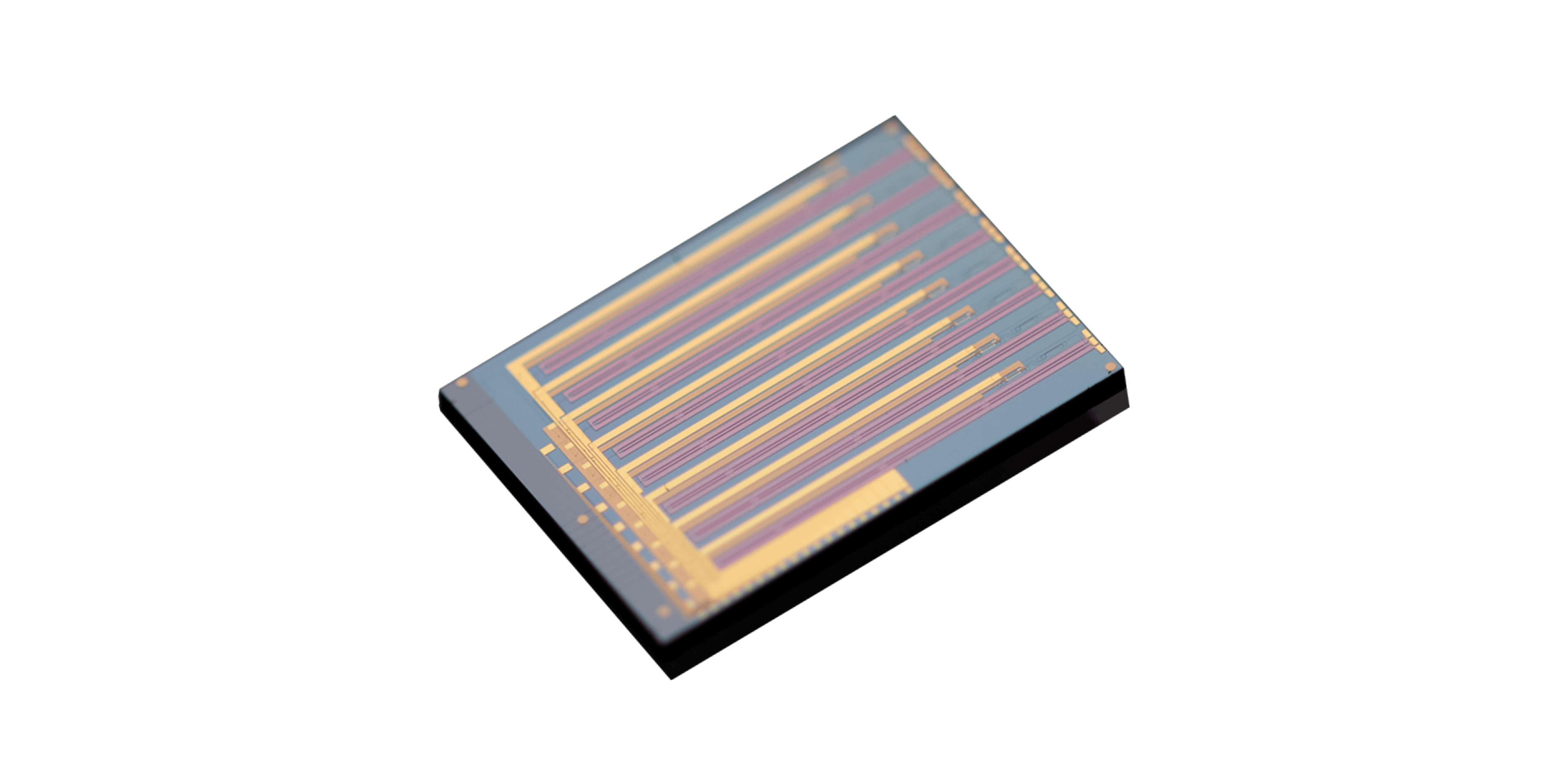
Electronic ICs have historically served as the backbone of data processing, yet they struggle as signal frequencies push into the sub-terahertz range. When we compare electronic systems to tfln chips, the primary difference lies in how data is encoded and transmitted. Electrical signals suffer from significant resistive loss and electromagnetic interference, which requires power-hungry amplification. Conversely, our tfln chips leverage the Pockels effect, allowing for high-speed modulation without the excessive heat generation typically associated with electronic components.
Our real-world testing demonstrates that we can achieve bandwidths exceeding 100 GHz. This level of performance is vital for modern data centers where power efficiency is a critical design metric. By reducing the half-wave voltage to sub-1V levels, our modulators operate directly with standard CMOS circuits, effectively eliminating the need for bulky, inefficient RF driver amplifiers.
Optimizing Performance for Challenging Environments
Beyond the data center, the transition from purely electronic ICs to hybrid photonic platforms is reshaping how we approach sensing in autonomous vehicles. In these environments, reliability and signal integrity are non-negotiable. Optical chips provide a significant reduction in footprint and power consumption compared to traditional electronic counterparts. By integrating multiple functionalities—such as lasers, modulators, and detectors—onto a single substrate, we create more robust systems that handle the rigors of real-time environment mapping.
We have found that the high linearity and thermal stability of our optical chips make them ideal for frequency-modulated continuous-wave (FMCW) LiDAR systems. These systems require precise beam steering, which our platforms achieve through solid-state, high-speed phase shifting. Unlike electronic systems that may require complex thermal management to maintain accuracy, our integrated solutions maintain stable performance across varying operational temperatures, ensuring consistent data throughput for mission-critical sensing tasks.
Practical Considerations for Next-Generation Design
When we evaluate the trade-offs between electronic ICs and photonic integration, the choice often hinges on the need for scalability and efficiency. Our research and development efforts are dedicated to bridging the gap between experimental laboratory successes and large-scale commercial deployments. By adopting 8-inch wafer manufacturing processes, we ensure that the performance benefits of our photonic solutions are accessible for mass production.
We recognize that engineers need components that integrate seamlessly into existing architectures while providing the headroom for future bandwidth requirements. Through our specialized fabrication techniques, we provide the tools to overcome the bottlenecks of traditional electronic design, enabling a transition toward faster, cooler, and more reliable communication infrastructures. As we continue to refine our designs, we remain focused on solving the technical hurdles that prevent the widespread adoption of high-speed optical links, providing reliable, energy-efficient solutions for our partners.


 The previous article
 Returns the list