Industry requirements for data bandwidth are growing, forcing engineers to compare different hardware foundations for high-speed systems. At Liobate, we often discuss the specific trade-offs between various material platforms, as the choice of substrate directly influences the performance of complex communication and sensing architectures. While silicon photonics provides massive scalability through established manufacturing processes, it encounters physical limits when tasked with ultra-high-speed modulation. Our research indicates that integrating thin-film lithium niobate (TFLN) offers a way to overcome these hurdles, providing a path toward 1.6T and 3.2T data rates.
The Material Physics of High-Speed Modulation
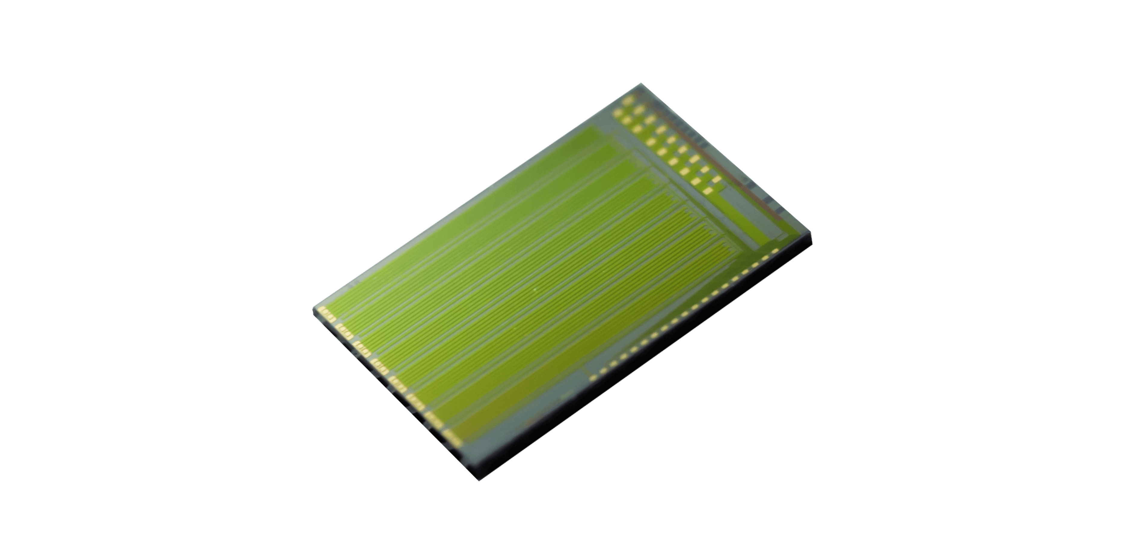
When we examine the fundamental mechanisms of light modulation, the differences between material platforms become clear. Silicon photonics typically relies on the free-carrier dispersion effect, which introduces inherent constraints on speed and energy efficiency. In contrast, TFLN technology utilizes the Pockels effect, which allows for linear, high-speed modulation without the significant power-hungry limitations associated with carrier-based designs. Our internal testing shows that the TFLN chip can provide bandwidth of 67 GHz and above for TFLN modulator chips, supporting optoelectronic oscillators, polarization measurement and control, frequency identification, etc., and is suitable for device-level and system-level solutions.. This physical advantage is crucial for supporting modern signal formats like 130 Gbaud PAM8, which are becoming standard in high-end data center interconnects.
Strategies for Heterogeneous Integration
Instead of viewing these platforms as mutually exclusive, we focus on how they can work together. Many developers are interested in how to combine the routing efficiency of silicon with the superior electro-optic performance of lithium niobate. At Liobate, we utilize heterogeneous integration techniques—such as wafer-scale direct bonding and micro-transfer printing—to place high-performance modulation layers exactly where they are needed. By utilizing standard silicon or silicon nitride substrates for passive routing while keeping the active modulation on a TFLN layer, we create high-density optical chips that provide the required signal integrity for demanding environments like autonomous driving and long-haul transport networks.
Solving Technical Challenges for Customers
Our partners often face a "power wall" when designing systems for AI clusters, where energy consumption and thermal output are primary constraints. The use of tfln chips addresses this directly, as the reduced half-wave voltage allows for drive voltages under 1.5 V. This design efficiency translates into exceptional energy savings per bit, helping our customers reduce the thermal load of their systems without sacrificing data throughput. By implementing these specialized components, we help our customers reduce the thermal load of their systems without sacrificing data throughput. Furthermore, these integrated solutions enable more compact form factors, which is essential for equipment manufacturers looking to pack higher density into limited rack space.
Reliable Performance in Demanding Applications
System reliability remains a priority for any deployment in optical communication or sensing. Our work with optical chips emphasizes repeatability and thermal stability, ensuring that performance remains consistent even during intense operations. We have verified these results through rigorous wafer-level statistical analysis, confirming that our fabrication methods deliver the yield and uniformity necessary for commercial production. As data demands continue to escalate, the ability to rely on mature, high-performance photonic components becomes a major strategic asset for any engineering team. We remain committed to providing the hardware foundations that enable reliable and efficient performance for future technical infrastructures.


 The previous article
 Returns the list