As we navigate the demands of 2026, the global appetite for data bandwidth and ultra-low-latency processing has pushed traditional silicon photonics to its physical limits.
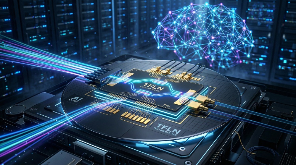
To break the "power wall" in AI clusters and 1.6T networking, the industry is turning its attention to thin-film lithium niobate (TFLN). This breakthrough material platform enables the fabrication of high-performance photonic integrated circuits (PICs) with unprecedented electro-optic efficiency.
What is Thin Film Lithium Niobate (TFLN)?
Technically referred to as lithium niobate on insulator (LNOI), thin film lithium niobate represents a fundamental architectural shift from traditional bulk lithium niobate components.
While the legacy industry relied on thick, ion-diffused crystals, TFLN utilizes a "sandwich" structure: a single-crystal lithium niobate thin film (typically 300 nm to 700 nm thick) bonded to a handle substrate like silicon, quartz, or sapphire via a low-refractive-index buffer layer, usually silicon dioxide (SiO₂).
This nanophotonic approach capitalizes on a high refractive index contrast (nₒ ≈ 2.2 at 1550 nm), allowing for a sub-micron mode field area. Unlike bulk crystals, TFLN supports sophisticated waveguide designs, including monolithic ridge waveguides formed by dry etching or rib-loaded structures where materials like SiN or TiO₂ are deposited onto the LN film.
This structural evolution allows for much tighter integration and significantly smaller chip footprints than were ever possible with legacy LN technology.
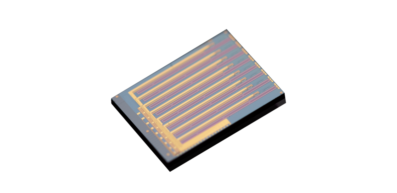
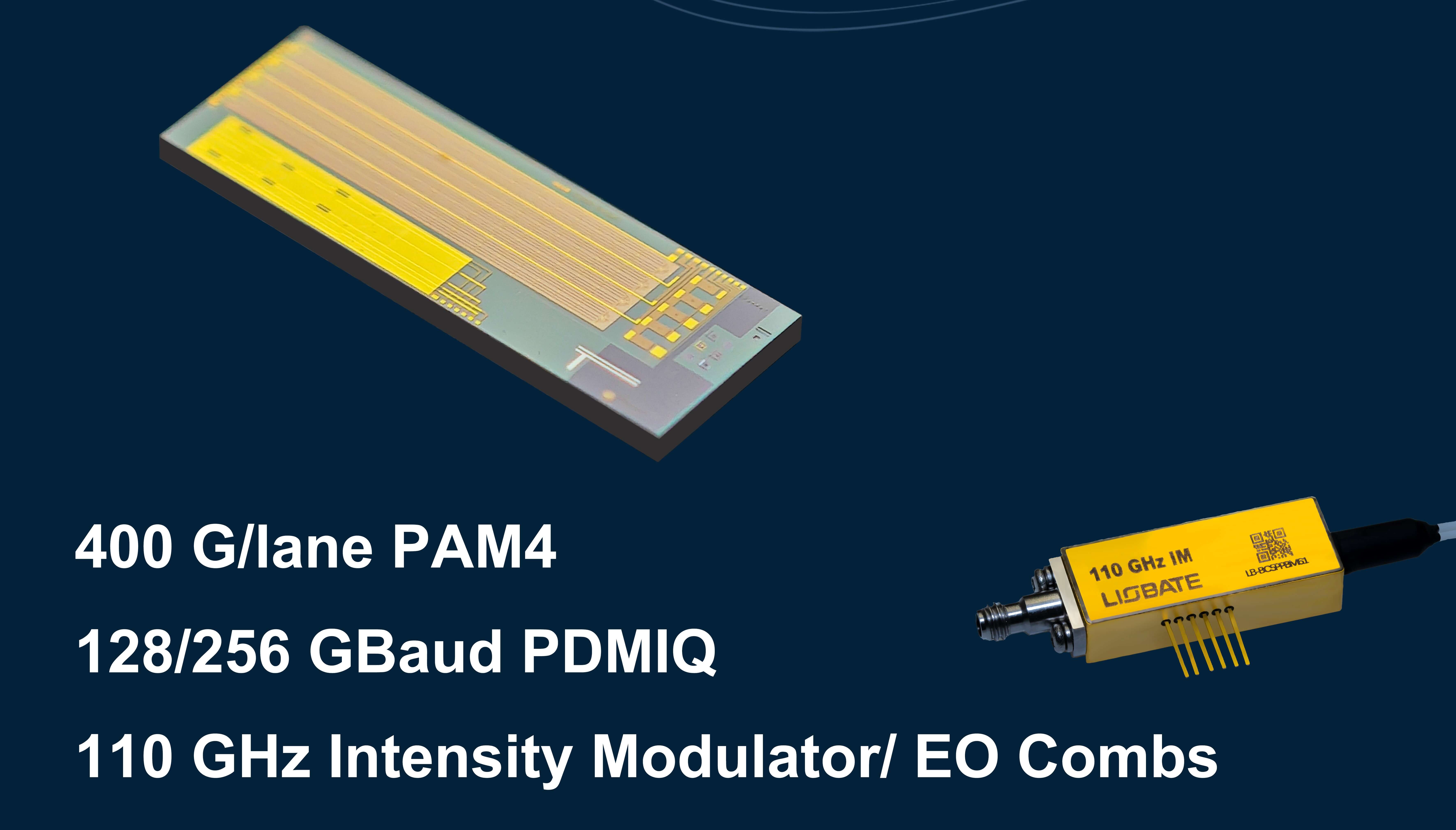
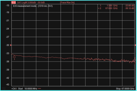
Picture shown: Liobate 3.2T DR8
Major Advantages of TFLN Chips
The attention drawn to TFLN is due to four critical performance pillars that address the bottlenecks of next-generation hardware.
1. Unmatched Speed
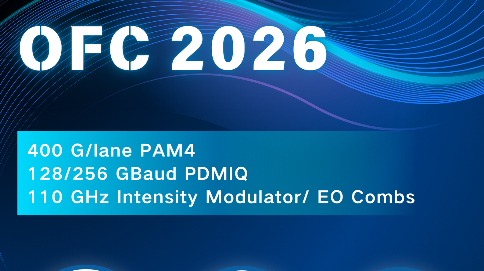
The standout feature of this platform is the thin film lithium niobate modulator. Thanks to the high Pockels coefficient (r₃₃ ≈ 31 pm/V) and the ability to achieve perfect velocity matching between microwave and optical waves, TFLN modulators now routinely exceed bandwidths of 100 GHz. In leading-edge laboratory and pilot-line settings, bandwidths reaching 220 GHz have been demonstrated, providing the necessary foundation for single-wavelength 1.6 Tbps and 3.2 Tbps transmission rates.
2. Extreme Energy Efficiency
In the era of hyperscale AI, power consumption is a primary constraint. TFLN waveguides offer exceptional modal overlap, which translates to a very low half-wave voltage (Vπ < 2V, with some designs achieving sub-1V). This allows the modulator to be driven directly by CMOS electronics without the need for power-hungry driver amplifiers. The energy consumption of these links can be as low as 0.69 fJ/bit, a transformative figure for green data center initiatives.
3. Scalability
A common critique of lithium niobate in the past was its "cottage industry" scale. However, as of 2026, the industry has gradually transitioned from 4-inch and 6-inch wafers to 8-inch (200 mm) wafer manufacturing. This shift can reduce the per-die cost and increase throughput, making TFLN a viable candidate for high-volume commercial deployments alongside traditional semiconductor materials.
4. CMOS Production Compatibility
Through wafer-level bonding and micro-transfer printing, modern TFLN can be integrated as a "back-end" process onto standard silicon photonics (SiPh) platforms. This allows designers to combine the superior modulation of LN with the established routing and laser integration capabilities of silicon and indium phosphide.
Who Can Benefit from TFLN Chips?
The versatility of the TFLN platform makes it a critical asset for several high-growth sectors:
1. AI and Hyperscale Data Centers: As AI models grow, the interconnects between GPUs require massive bandwidth. TFLN modulators solve the "power wall" by enabling 800G and 1.6T optical transceivers with minimal thermal output.
2. Telecommunications (6G Ready): TFLN is an important engine for 6G photonics, capable of covering the spectrum from microwave to sub-terahertz (THz) frequencies while maintaining ultra-low phase noise.
3. Quantum Technology: The strong second-order nonlinearity (d₃₃ ≈ -27 pm/V) is ideal for generating squeezed light and entangled photon pairs, essential for Quantum Key Distribution (QKD) and quantum computing.
4. LiDAR and Sensing: The fast phase-shifting capability allows for all-solid-state beam steering, which is vital for high-resolution, long-range LiDAR in autonomous vehicles.
Challenges and Solutions for TFLN Chip Manufacturing
Although TFLN offers numerous advantages, its manufacturing still faces challenges in scaling up and bottlenecks in the supply chain. However, the future of thin film lithium niobate chips still remains promising.
1. Fabrication Complexity
TFLN fabrication faces significant hurdles regarding etching difficulty and CMOS compatibility. Since Lithium Niobate is chemically stable, standard dry etching often results in sidewall roughness and byproduct redeposition, which degrades device performance.
To overcome this, the industry utilizes a diverse technical matrix. For instance, rib-loaded waveguides avoid direct etching by patterning easier materials on top of the TFLN, while photolithography-assisted chemo-mechanical etching (PLACE) uses polishing to achieve ultra-low loss. Other techniques like atomic layer etching (ALE) and heterogenous integration (BEOL) are also vital in bridging the "fabrication gap."
2. Supply Chain Stability
The TFLN supply chain is currently constrained by limited high-quality wafer production, small wafer sizes (3–6 inches), and a lack of commercial foundries. To resolve these bottlenecks, the industry is shifting toward 8-inch wafer production to leverage existing semiconductor infrastructure and reduce unit costs.
Simultaneously, organizations like QCi and CSEM are establishing specialized TFLN foundries while offering standardized Process Design Kits (PDKs). These strategies, alongside global supply diversification and MPW services, represent a broader ecosystem effort.
Liobate: Leading the TFLN Revolution
Liobate is a high-tech enterprise dedicated to developing thin-film lithium niobate modulator PICs and high-performance optical sub-assemblies. Led by world-renowned expert Prof. Cai Xinlun, our technical team leverages years of R&D to provide mass-production-ready solutions. Our core capabilities include:
• Record-Breaking Performance: We offer TFLN modulators achieving sub-1V driving voltages and bandwidths over 110 GHz, supporting 800G to 3.2T IMDD applications.
• Proprietary Stability Technologies: We have developed multiple proprietary technologies, including the technology that successfully eliminates the "bias drift" effect, ensuring highly stable and repeatable DC operation—a critical breakthrough for commercial reliability.
• Full-Stack PIC Integration: Our platform supports the monolithic integration of ultra-low loss waveguides, micro-resonators, and multi-channel modulators for high-density applications.
• Global Market Reach: Through strategic collaborations, we provide high-speed optical chips and modules—such as 128GBaud PDM-IQ chips and 67/110 GHz ultra-high bandwidth modulators—tailored for hyperscale data centers, communication networks, high-precision test instruments, and autonomous driving (autopilot) systems.
Conclusion
In summary, thin film lithium niobate represents a transformative leap in photonic technology, offering unmatched speed, energy efficiency, and scalability for AI, telecom, quantum, and sensing applications.
Liobate’s expertise ensures high-performance, production-ready TFLN solutions. To explore how these innovations can elevate your projects, reach out to Liobate today and discover the future of optical integration!
Relevant information:
1. https://www.photonics.com/Articles/The-Return-of-Lithium-Niobate-From-Bulk/a71688
2. https://www.researching.cn/ArticlePdf/m00090/2022/4/3/034003.pdf
3. https://www.universitywafer.com/thin-film-lithium-niobate-applications.html
4. https://www.neoncq.com/how-thin-film-lithium-niobate-modulators-are-manufactured
6. https://www.researching.cn/ArticlePdf/m00005/2024/22/9/090003.pdf
7. https://pubs.aip.org/aip/app/article-pdf/doi/10.1063/5.0230797/20341177/016105_1_5.0230797.pdf

 The previous article
 Returns the list