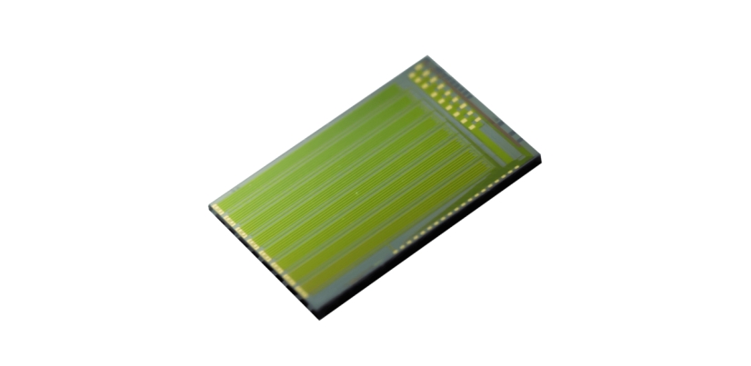
Integrated photonic chip technology is constantly iterating and maturing, and its comprehensive performance directly affects the construction quality of modern optical communication systems. To help industry users make reasonable selection and deployment decisions, we objectively sort out the advantages and existing limitations of current mainstream integrated photonic chips, taking our multi-functional TFLN photonic chip as a practical research case.
Advantages of Integrated Photonic Chips
One of the most significant benefits of integrated photonic chips, such as our TFLN chips, is their ability to support high-density photonic integrated circuits. This feature is crucial for maximizing efficiency in AI and cloud data center optical modules. The low insertion loss of less than 14 dB, including coupling loss, ensures that data integrity is maintained throughout the transmission process.
Moreover, the half-wave voltage of less than 2 V is a decisive factor for energy efficiency, making these optical chips not only cost-effective but also environmentally friendly. They operate effectively in various conditions, supporting both AC and DC coupling, which enhances their versatility across multiple applications.
The integration of these chips simplifies system designs, allowing for faster deployment and reduced manufacturing complexity. By consolidating functions into a single chip, the reliability of the overall system improves, which is critical for demanding environments like data centers.
Challenges and Limitations
Despite their advantages, there are notable challenges associated with current integrated photonic chips. For one, the technology is still relatively nascent, which can lead to limited availability and higher costs compared to traditional semiconductor solutions. These initial investment barriers can deter organizations from making the switch to integrated optical chips.
Temperature sensitivity is another concern. While our TFLN chips are designed to operate within specified parameters, fluctuations in temperature may affect performance, especially in applications requiring stringent environmental controls. This necessitates robust thermal management solutions, adding complexity to the overall system design.
Additionally, interoperability with established infrastructure poses challenges. Organizations may encounter difficulties integrating these advanced optical chips into existing systems, which can slow down adoption and increase the overall implementation timeline.
Moving Forward in Optical Technologies
As we continue to innovate in the field of integrated photonic chips, it's essential for industry players to weigh the pros and cons objectively. The advancements we bring to the table, particularly with Liobate's TFLN chips, are setting new benchmarks in performance and efficiency. Yet, understanding the challenges allows us to better prepare for the future.
By fostering collaboration across the industry and investing in R&D, At Liobate, we can address existing limitations and unlock the full potential of optical chips. The future of integrated photonic technology is bright, and together, we can pave the way for its rapid adoption and transformative impact on data centers and beyond. Balanced pros-and-cons evaluations can draw on customized TFLN modulator measurements, whitepaper resources, and sample evaluation sessions arranged by Liobate's engineers.


 The previous article
 Returns the list