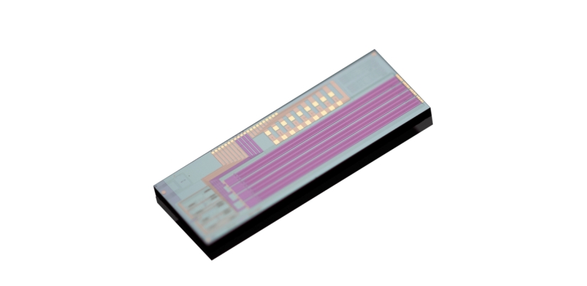
At Liobate, we are deeply committed to advancing the future of optical technology while being mindful of our environmental responsibilities. Our TFLN photonic chip, specifically designed for long-reach coherent transmission, exemplifies this commitment. By supporting polarization-division multiplexed IQ modulation with a remarkable 70GHz bandwidth for both 800G and 1.6T ZR modules, we are not only enhancing data capacity but also working towards significant carbon footprint reductions.
The Environmental Benefits of TFLN Chips
The TFLN photonic chip offers several eco-friendly advantages that contribute to reduced carbon emissions in the data transmission process. First and foremost, our chip features an insertion loss of less than 7 dB, which translates to higher operational efficiency. This efficiency means that less energy is consumed during transmission, leading to a considerable decrease in the overall carbon footprint associated with data processing and communication.
Additionally, the half-wave voltage of less than 4.5 V enhances the chip's power efficiency, allowing devices to operate with lower energy requirements. By minimizing power consumption, TFLN chips help in decreasing the demand on power plants, many of which rely on fossil fuels. As organizations seek to meet sustainability goals, incorporating these advanced optical chips into their systems can play a crucial part in their carbon reduction strategies.
Assessing Carbon Footprint Reduction Metrics
To measure the carbon footprint reduction achieved through the adoption of TFLN photonic chips, we can evaluate specific metrics. Key performance indicators (KPIs) include the reduction in energy consumption over time, the efficiency of signal transmission, and the longevity of equipment life span.
By analyzing the energy savings associated with TFLN chips, we can provide concrete data illustrating how organizations can reduce their total greenhouse gas emissions. For example, a data center transitioning from traditional optical technologies to our TFLN photonic chip can expect to see lower operational costs due to energy efficiency while simultaneously contributing to broader sustainability initiatives.
Furthermore, the low insertion loss of our TFLN chip also leads to less heat generation. This not only improves the performance of cooling systems but also extends the lifespan of the equipment, resulting in less electronic waste and further contributing to a reduced carbon footprint.
Paving the Path to Sustainable Solutions
Liobate is dedicated to ensuring that our TFLN photonic chip not only meets the demands for high-speed data transmission but also aligns with the urgent need for sustainable practices. As we move forward, we will continue to innovate and refine our technologies to further enhance their environmental benefits.
By prioritizing eco-friendly solutions, we can help organizations achieve their sustainability goals while revolutionizing the optical chip landscape. Together, we can champion a future where advanced technology and environmental stewardship go hand in hand, ensuring that our legacy is one of responsible innovation and reduced carbon footprints. Carbon-footprint studies can be paired with project-specific TFLN modulator test data, technical papers, and sample evaluation guidance from the engineering team.


 The previous article
 Returns the list