Safety and precision define the way we interact with advanced hardware in our research facilities. At Liobate, we manage high-power optical systems by prioritizing standardized workflows that protect both our personnel and our sensitive components. Because tfln chips utilize high-intensity light for high-speed data transmission, the risk of accidental exposure or device damage is a concern we address through rigorous operational protocols. By treating every optical connection as a potential source of high-energy output, we create a secure environment where innovation can proceed without interruption.
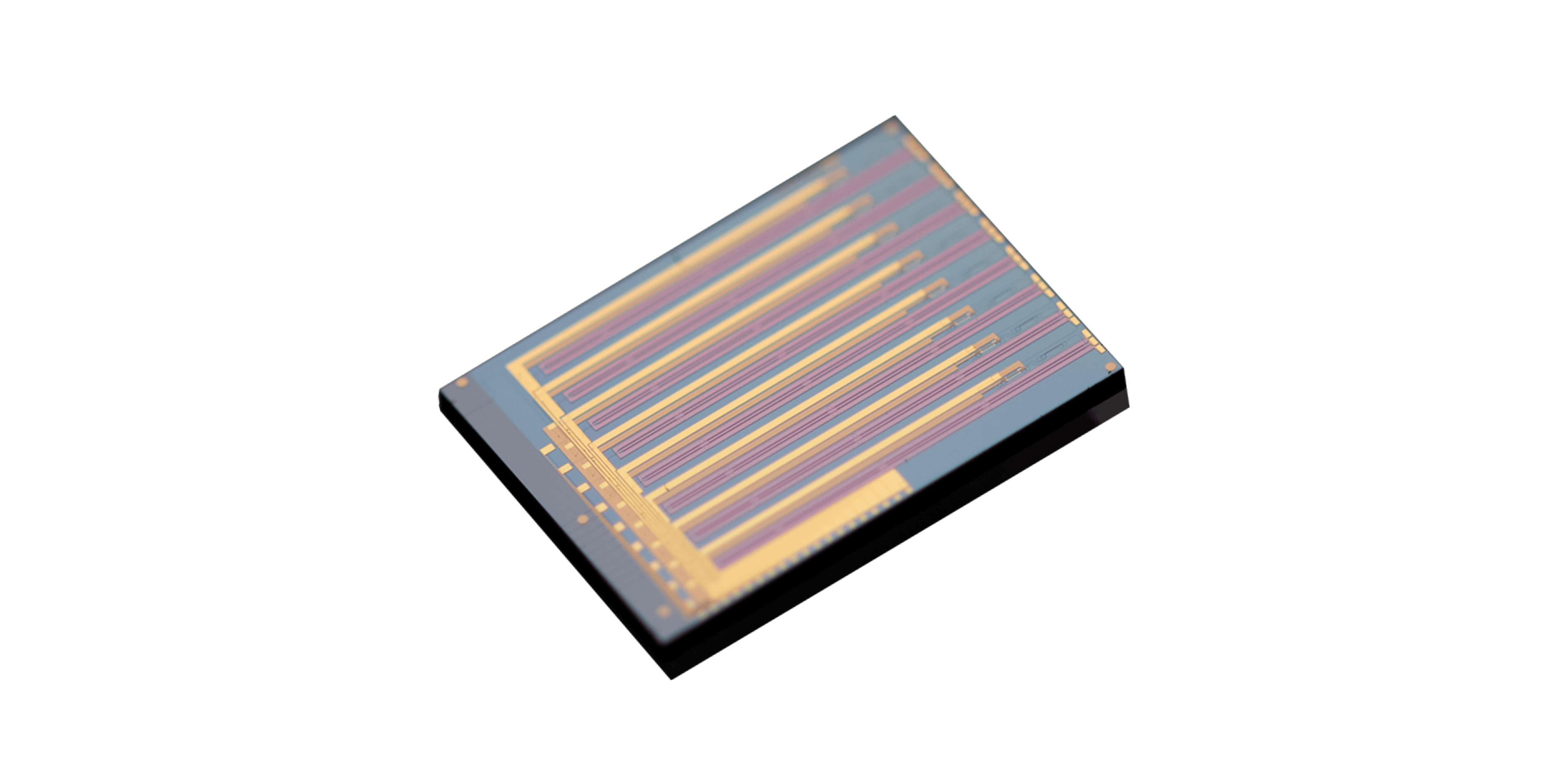
Operational Safety for Integrated Photonic Chips
Personal protection is the first line of defense when we operate laser-coupled systems. We mandate the use of eye protection designed for the specific wavelengths emitted by our integrated photonic chips. Since these components can achieve high optical power densities, even minor reflections can pose risks if proper barriers are not in place. Our lab setup includes light-tight enclosures for all test benches, ensuring that stray light is contained at the source. When we verify our experimental configurations, we double-check these shields to confirm that they provide adequate attenuation before powering on any laser sources.
Beyond individual safety, we focus on the integrity of the hardware itself. High power levels can lead to thermal accumulation if the coupling between the fiber and the chip is not optimized. We perform all alignments with low-power pilot beams to confirm stability before ramping up to operational levels. By monitoring the thermal output of our tfln chips during these transitions, we prevent potential damage to the delicate waveguide structures. This gradual approach allows us to confirm that our mounting solutions, which are designed for efficient heat dissipation, are functioning as expected during high-power trials.
Preventing Damage to Advanced Photonic Circuits
Contamination is a frequent cause of component failure in photonics. We store all integrated photonic chips in cleanroom-compliant packaging when they are not in use to prevent dust or debris from settling on the optical facets. When it comes time to connect these devices, we utilize automated inspection scopes to ensure that every interface is pristine. If we notice any particulate matter on the facets, we employ controlled cleaning methods rather than manual wiping, which can scratch the surface. This care is essential because even microscopic damage can absorb significant energy, leading to localized heating that can permanently degrade performance.
We also pay attention to the mechanical stress applied during cable connections. We utilize custom jigs that provide strain relief, ensuring that the alignment of the fiber remains stable over long periods. As we push the boundaries of what our systems can achieve, we find that the combination of strict environmental controls and careful handling results in a higher success rate for our experiments. By adhering to these practices, we ensure that the high performance we demand from our devices is never compromised by avoidable errors in the laboratory setting.
Consistency in Laboratory Workflows
Consistent results depend on the discipline of the individuals performing the tests. At Liobate, we train every team member on the specific requirements of our photonic platforms, emphasizing that caution is necessary even when using small-scale components. We record the power thresholds and thermal profiles for each device to build a library of performance data that guides our future work. This documentation helps us recognize when a device might be reaching its limits, allowing us to adjust our procedures before reaching a failure point. We are committed to fostering a culture where technical excellence and safety are viewed as parallel goals. Through these refined methods, we support the ongoing development of faster and more efficient optical communication systems.


 The previous article
 Returns the list